Laser cutting enables faster machining times and is replacing conventional mechanical cutting, stamping and milling. Conventional methods typically perform poorly when tolerances are ±0.1 mm, and also have to have post-processing, whereas fiber and CO2 lasers can easily hold tolerances down into the micron range with minimal heat-affected zones. This eliminates secondary finishing processes, which shortens production times by as much as 40 percent for automotive applications.
As laser processing is a non-contact process, the material can be manipulated easily without costly tooling changes. laser systems now machine titanium aircraft components and engrave microelectronics with no mechanical clamps, saving 30% of material. Industrial laser systems can cost more than $500k, but with an average 18-month payback period based on energy savings and scrap reduction for manufacturers.
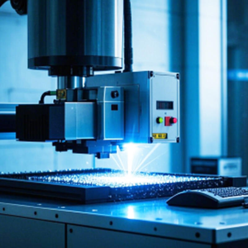
Modern electronics manufacturing relies on three core laser technologies—CO2, fiber optic, and solid-state—each addressing distinct production challenges.
Non-metallic processing is typically performed with CO2 lasers, which have a 10.6 μm wavelength that readily interacts with organic materials. These systems mark polymer-based circuit board substrates and cut acrylic device housings at rates of up to 2m/s and we have industrial data that demonstrates CO2 technology has 38% market share in packaging for consumer electronics. Their plastic-and ceramic-compatibility makes them well-suited for connector, insulator, and RFID tag antenna applications.
Fiber lasers excel in processing conductive materials like copper and aluminum. Their 1.06 μm wavelength achieves 20 μm cutting precision with 30% less energy consumption than CO2 alternatives. Manufacturers use 500W-1kW systems to produce EMI/RF shielding components, achieving dross-free edges on 0.5 mm stainless steel sheets.
Solid-state lasers enable micron-scale welding of battery terminals and sensor components without damaging heat-sensitive parts. Pulsed Nd:YAG systems produce 0.1 mm weld seams on copper-nickel alloys used in micro-USB ports, maintaining joint conductivity above 90% IACS.
Fiber lasers achieve marking speeds exceeding 10 m/s while maintaining ±5 μm accuracy, critical for high-density interconnect designs. Laser-marked traces reduce short-circuit risks by 37% compared to chemical etching methods. Automated vision-guided systems self-correct alignment errors in real-time, particularly valuable for flexible PCB substrates.
UV laser systems (355 nm wavelength) enable sub-50μm feature engraving essential for micro-BGA packages. This cold ablation process prevents thermal damage to adjacent copper layers.
Multi-layer PCB construction uses pulsed fiber lasers for precision dielectric removal, exposing buried vias without compromising adjacent 18μm copper layers.
Green lasers solve challenges with reflective metals like copper and gold by operating at 532 nm wavelengths where copper absorbs 40% more energy.
Reflective metals pose two primary obstacles:
Modern systems address these through pulsed operation and nitrogen gas assist, reducing kerf widths by 58% compared to CO2 laser cutting.
A manufacturer transitioning to green lasers achieved:
| Metric | Improvement |
|---|---|
| Edge roughness | 0.8 – 0.2 μm |
| Production throughput | +22% |
| Scrap rate | -40% |
AI optimizes laser parameters by analyzing over 300 data points per second, reducing defects by 35%. Machine learning adjusts beam focus in real-time, achieving 99.7% consistency in micro-welding operations.
Networked laser systems predict failures 72 hours in advance, extending laser tube lifetimes by 200–300 operational hours.
Ultrafast lasers enable processing below 500 nanometers, reducing thermal damage by 60–80% compared to conventional methods.
Next-gen systems integrate cutting, welding, and surface treatment, reducing cycle times by up to 40% while maintaining micron-level accuracy.
Laser technology offers faster machining times and higher precision, which reduces the need for secondary finishing processes. It also facilitates energy savings and material efficiency.
CO2, fiber optic, and solid-state lasers are commonly used, each suited to different materials and applications.
Laser technology enables precise marking and ablation of PCB components, improving production speed and reducing errors.
Green lasers operate at wavelengths where reflective metals like copper absorb more energy, reducing energy loss and thermal spread.
Shandong ZhongGuangDian provides advanced laser marking machines and custom laser equipment for various industries. Our reliable products, fast delivery, and lifetime warranty ensure customer satisfaction.